DiUS has designed, developed and manufactured devices for the Smart Energy (SE) market and the broader Internet of Things (IoT) eco-system since 2009.
With our advanced Smart Meter roll out, we focused our SE activities in Victoria. Recently, a potential opportunity came up to trial an SE solution outside of Victoria where there was a very limited number, or no Smart Meters deployed and we didn’t have a simple solution we could offer.
As a result, we undertook to develop a device that could be used in small to medium proof-of-value (PoV) trials across all states in Australia. Combined with an off the shelf in-line power meter, the new device would act as a Smart Meter, enabling us to perform SE trials just like here in Victoria. Additionally, the device had to offer short development cycles when adding new features. Although unit cost was important, the time to develop new functionality was more crucial.
Our starting point was an obvious choice; the basis for the device would be a Raspberry Pi 2. Raspberry Pi hardware is readily available at a reasonable price. It has a huge and active open source community, thus giving great support. The flexibility of developing in a Linux environment coupled with an open source community meant that adding, for example WiFi was a simple exercise. Also, it’s possible to do a lot with a quad-core ARMv7 CPU running at 900MHz and 1GB of RAM.
The design consisted of a Pi 2 and a board we designed according to the Raspberry Pi’s Hardware-Attached-on-Top or HAT form factor. We designed the HAT printed circuit board so that it could be built with either a 2.4GHz ZigBee radio or a 900MHz 6LowPAN mesh radio module to make the unit generic and usable in both our SE and IoT applications.
Why did we choose the HAT form factor?
Well to start with, it’s really well defined both mechanically and electrically. We simply adopted the specification as is, which made the design much quicker and easier. The specification also included the use of an ID bus with an EEPROM for auto-detection of the HAT hardware. With software support, the Pi automatically loads the relevant drivers, thus effectively making the HAT a plug-n-play module.
What does the device do?
The combined unit (Pi+HAT) can be configured for different roles and perform a number of functions.
Here are some of its features:
- It acts as a gateway by bridging traditional interfaces such as WiFi (or Ethernet) to either ZigBee or 6LowPAN mesh radio networks, depending on the version of HAT hardware installed.
- It performs the role of an Energy Services Interface (ESI), just like a Smart Meter.
- It can be deployed as a remote sensor unit by attaching (in addition to the on-board light sensor chip) different sensor devices using general I/O or the Pi’s USB ports.
- The HAT specification also includes physical support for a Pi camera, turning the unit into a mesh capable remote camera.
We think the device is really cool; the Pi makes it easy to develop and gives us a highly customisable IoT platform to work with. Also, we can use the HAT with zero software configuration which makes it very easy to swap HATs. We now have something that can be easily used in the SE space outside of Victoria and also support IoT applications.
What does it look like?
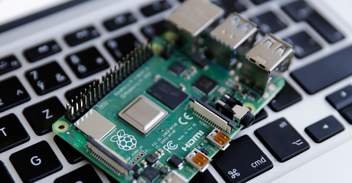
Shown below a picture of the unit without its plastic housing – you can see on the top of the Pi that the Hardware-Attached-on-Top, in this case the HAT is loaded with the 900 MHz 6LowPAN module.

Pi+HAT device
The device is small and measures:
- 85 x 55 x 20 mm for Pi + HAT
- 65 x 55 x 5 mm for HAT only
How did we develop the unit?
The unit was developed from initial design to working hardware in about five weeks; two weeks for the hardware design, schematic entry and printed circuit board (PCB) layout, three weeks for PCB fabrication, and one day for PCB assembly. Whilst we waited for the PCB, we procured all components needed to build the device.
The design process we used was split into four stages: schematic entry, PCB design, PCB fabrication and component procurement and PCB assembly. The schematic entry and PCB design stages were conducted in an agile fashion by including internal product owners and our business development manager, particularly in the early design stage. Changes from the reviews included the addition of a light sensor and the ability to flexibly allocate serial interfaces between the Pi and the HAT through the use of zero-ohm resistors on the PCB .
The schematic entry stage involved electronic hardware design and components selection. For rapid prototyping, it was crucial to select components based on stock availability. As PCB fabrication turn-around time is quite long, we spent considerable amount of effort to review and revise the schematic as errors or new requirements were identified.
Before proceeding to PCB layout, a PCB fabricator was selected first because manufacturing capabilities and constraints vary between different fabricators, which affects the layout. The mechanical design was also taken into consideration as it could have affected component placement and PCB size and shape. After all the constraints were identified, we then moved to PCB layout. In addition to a PCB design review, an actual-size layout printed on cardboard was used to verify the mechanical design and component footprints. We iterated between schematic entry and PCB design process multiple times before we were able to send it off to a PCB fabricator.
Then we went ahead and purchased all the required components. All we had to do then was to wait for the PCB and parts to arrive and assemble them.
What’s Next?
We are now at a point where we can consider what to do next. First up is to fix the strap wires – yes we got it wrong, but only four tracks that were easily fixed on the prototype. It’s very common to have multiple revisions of a PCB before you get it right!
We’d like to remove a sizable pin header (it’s no longer needed) which will free up room for other circuitry. We don’t need the JTAG header any longer as we can now program the HAT using the Pi.
We would also like to minimise power consumption so that the device can be more readily powered using a small battery and solar panel. For IoT applications, the Pi which happens to be relatively power hungry, does not need to be powered on all of the time. We plan to use the microcontroller from the 900 MHz 6LowPAN / ZigBee module (which is a low-power MCU) to control the power state of the Pi, this should considerably reduce the overall power consumption of the unit.
We will also consider adding other small footprint micro-electro-mechanical sensors (MEMS): humidity, accelerometer, pressure, digital compass, microphone, inertial module and potentially a gyroscope. Adding GPS capability so we can geolocate the unit is also on our list.
Finally, we don’t have a cool name for the unit. If you have something appropriate in mind we’d love to hear from you.
This article was co-written by Joo Aun Saw and Zoran Angelovski.